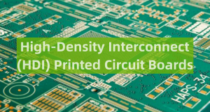
The Significance of Via Structures in HDI PCBs
Via Structures in HDI PCBs
A high-density circuit board requires high performance in a small package. This has been possible with HDI technology that allows for smaller components and shorter traces. The smaller traces reduce internal noise and increase signal strength and quality. Another important feature of HDI PCBs is the use of microvia structures. These tiny vias allow signals to travel a much shorter distance and they also eliminate stubs which can cause signal degradation.
The significance of a via structure in an hdi pcb is that it allows for more complex designs to be fabricated on the same piece of board. This is due to the smaller traces and the ability of microvias to connect all layers of the stackup. In addition to this, the smaller diameter of these vias also lowers parasitic loads and inductance which also contribute to a higher level of quality for the board.
Via structures are the means by which these connections are made between the copper elements on different layers of the PCB. The most common type of via is the through-hole (PTH) which is a hole that is drilled through the PCB and plated. These types of vias are used for a variety of purposes such as connecting components to the outside world or routing a net (a logical connection defined in the schematic).
The Significance of Via Structures in HDI PCBs
Another type of via is a blind microvia which is a small hole that is drilled into the copper layer and filled with a conductive epoxy. This via can be buried in the stack or it may be left unfilled to provide a flat surface on the top or bottom of the PCB. It can then be capped or filled with a metal to ensure good electrical contact.
Finally, there is the stacked or staggered microvia which is a series of blind or buried vias that are arranged in a stack on top of one another. This is a common way to bridge between layers in an HDI board. The microvias in the stack are then filled, capped and plated. The stacks are then heat pressed together in two stages.
It is important to keep in mind that the type and amount of vias, through-holes or microvias will have an impact on the cost of an HDI PCB. This is because these features require precision and can be time consuming to process. Additionally, the number of layers in the PCB will impact the price as well. For instance, a 6-layer HDI board with 2-n-2 construction will be more expensive than a 6-layer conventional non-HDI PCB.
The final note about via structures in HDI is that they need to be sized correctly to avoid the possibility of failure during manufacturing. This is because the manufacturing process of HDI PCBs involves a lot of laser drilling and precise alignment. This can be difficult to do if the PCB is too large for the available space. Therefore, it is essential to check with your manufacturer to make sure they have the capability of implementing an appropriate via structure for your specific design.